High-Fidelity 3D Nanoprinting of Plasmonic Gold Nanoantennas
D. Kuhness, A. Gruber, R. Winkler, J. Sattelkow, H. Fitzek, I. Letofsky-Pabst, G. Kothleitner and H. Plank
The interest in plasmonics and in particular in nano-plasmonics is still unbroken, due to their highly interesting physics and potential applications such as nano-emitters or high-performance sensors. Consequently, appropriate methods for a controlled and reliable fabrication of related structures are in demand. Although classical methods, such as resist-based approaches or fabrication from wet chemical processes, are well matured, they have intrinsic limitations such as the applicability to flat surfaces or the stochastic placement, respectively. In contrast, additive direct-write methods have the potential to overcome such limitations, although techniques for reliable sub 100 nm fabrication are only a few. In that context, Focused Electron Beam Induced Deposition (FEBID) is one of the promising candidates, as it not only meets resolution requirements but also allows true 3D nanoprinting (3D-FEBID) on a broad range of materials and on most surface morphologies as long as accessible by the e-beam.
Shape evolution and growth mechanisms of 3D-printed nanowires
R. Winkler, J. D. Fowlkes, P. D. Rack, G. Kothleitner and H. Plank
With our previous works, we have re-pioneered 3D-nanoprinting using focused electron beams (3D-FEBID), which finally allows the fabrication of even complex geometries (Fig. 1a). The physical properties of such free-standing structures are determined by the dimensions of constituent nanowires. However, little knowledge is available about their exact shape, which is indispensable for calculations and simulations as well as for optimization in applications. In a comprehensive study, which was published in Additive Manufacturing, we studied the shapes of freestanding segments as function of inclination angles, primary electron energy, beam currents, and precursor flux. While wire widths are monotonically increasing with segment angle, the thicknesses reveal distinct maxima at medium inclinations for higher primary energies. Furthermore, the study focused on the on-axes evolution of cross-sectional shapes and cross-sectional areas, which revealed super-elliptical shapes.
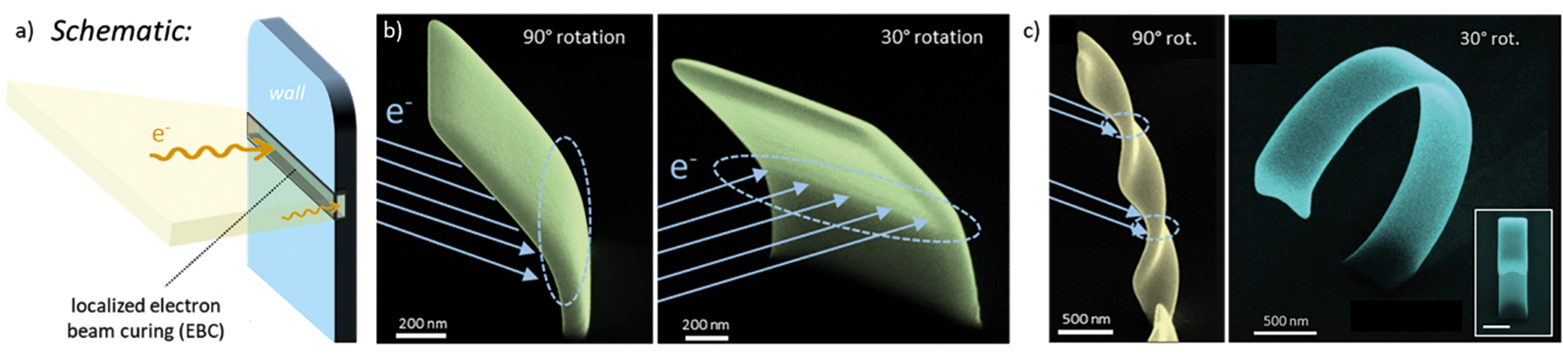
Controlled Morphological Bending of 3D-FEBID Structures via Electron Beams
A. Weitzer, R. Winkler, D. Kuhness, G. Kothleitner and H. Plank
In our previous work we made an important contribution to building closed or sheet-like 3D FEBID elements on a highly precise level in a reproducible way. Our next goal was to use the post-growth approach of Electron Beam Curing (EBC) to morphologically and functionally alter such structures. This technique, once again, exposes already deposited FEBID architectures to electron beam radiation, this time without precursor gas present. Thereby, the method proceeds with the dissociation of molecules that were incompletely fragmented in the FEBID process and incorporated into the deposited material. Although already known for several years, EBC was so far mainly used for changing the inner structure of entire FEBID elements, primarily concerning their carbon content. Thereby, often undesirably, the overall shape of the structures was altered in the process due to uneven volume loss. Here, it was used in a localized way, by irradiating only limited areas of 3D-FEBID structures to trigger specific deformations.
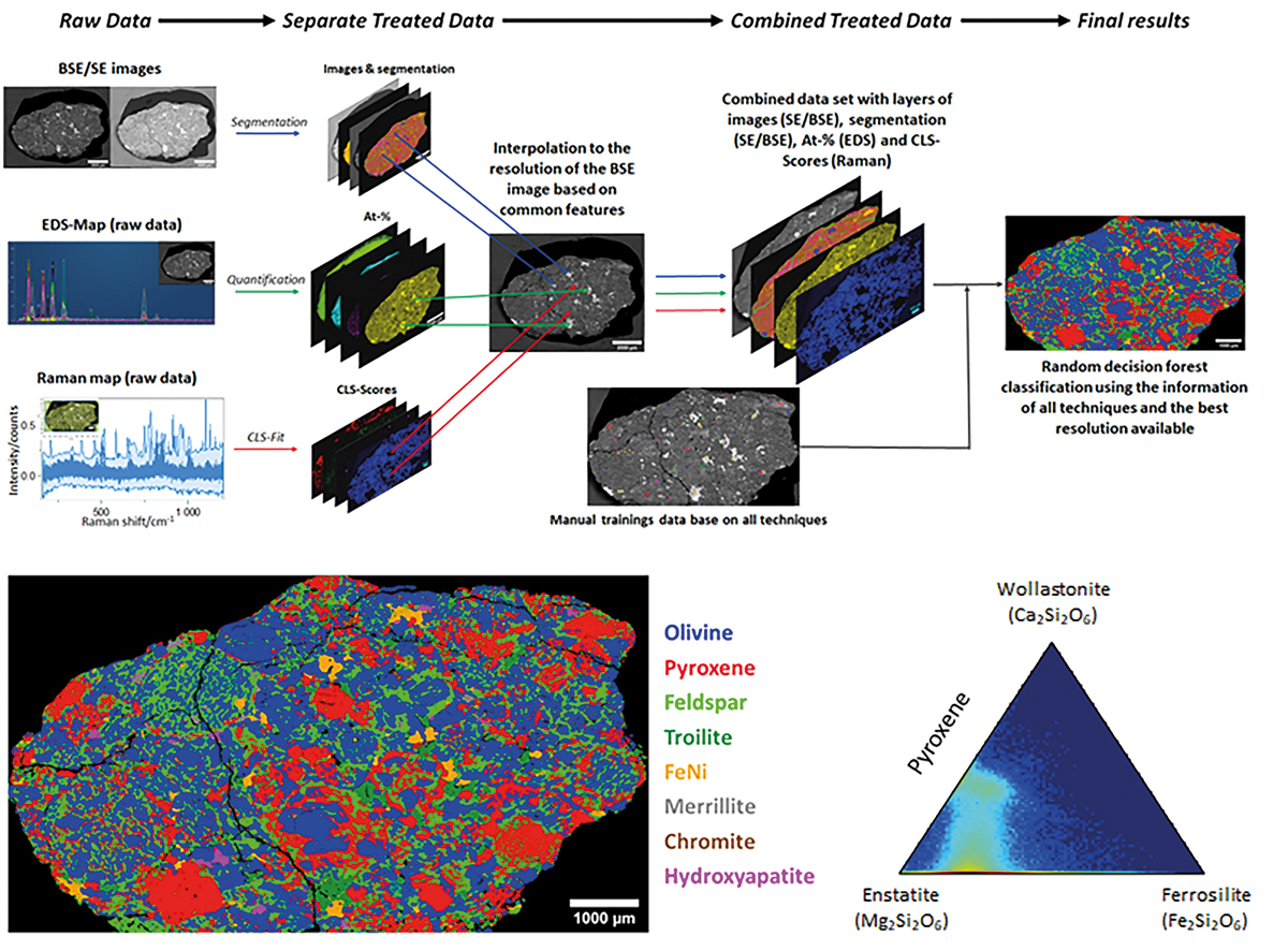
Correlating whole sample EDS and Raman mappings – A case study of a Chelyabinsk meteorite fragment
Harald Fitzek, Armin Zankel, Martina Dienstleder, Johannes Rattenberger, Hartmuth Schröttner, Ferdinand Hofer
Meteorites contain unique phase and structures over a wide range of sizes. Identifying and mapping these phases correctly requires as broad a range of analytical tools as possible, as well as high-resolution, yet large area, microscopy. The combination of Raman and EDS, which has been pioneered by the FELMI-ZFE in recent years, can provide a good toolbox for both crystallography (Raman) and composition (EDS). However, large area mappings with these techniques tend to have somewhat limited resolution. It is possible to do large area SEM images (SE/BSE) with good resolution of course, but these lack the analytical insights of Raman and EDS.
Therefore, in this work we combined whole sample Raman/EDS-mappings and SEM images into a single dataset. This allows us to preserve all the advantages of every individual technique, whilst using machine-learning algorithms to generate uniquely detailed phase mappings and gain additional insights.
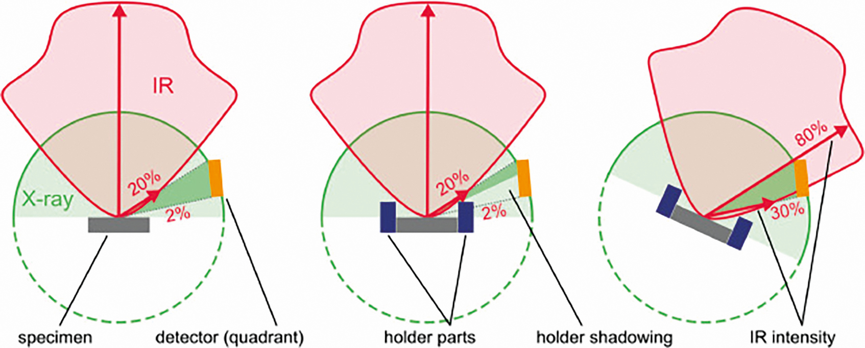
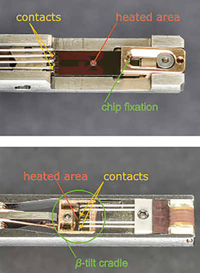
The Performance of EDXS at Elevated Sample Temperatures Using a MEMS-Based In Situ TEM Heating System
R. Krisper, J. Lammer, Y. Pivak, E. Fisslthaler, W. Grogger
Since the development of MEMS heating holders, dynamic in-situ experiments at elevated temperatures may be complemented by X-ray spectrometry for chemical analysis. Although the amount of IR radiation is small when compared to furnace holders, the influence of IR radiation emitted from the heating device on the quality of the X-ray spectra is significant. In this work, we systematically examine the influence of infrared (IR) radiation generated by MEMS-based in situ heating systems (DENSsolutions single- and double-tilt holders) on the results and interpretation of energy-dispersive X-ray (EDX) spectra through simulation and measurement. Focal points of interest in this study are the influence of holder geometry, shadowing and orientation with respect to the different emission characteristics of IR and X-ray photons and their interaction with a side-entry and a multi-detector system.
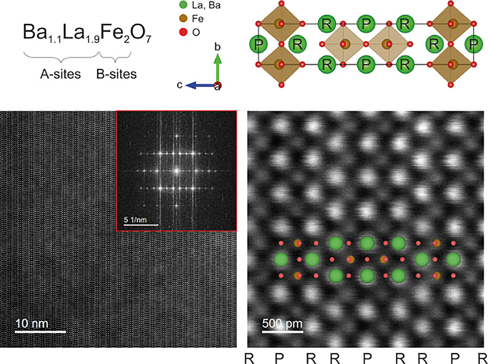
A method for a column-by-column EELS quantification of barium lanthanum ferrate
J. Lammer, C. Berger, S. Löffler, D. Knez, P. Longo, G. Kothleitner, F. Hofer, G. Haberfehlner, E. Bucher, W. Sitte, W. Grogger
High-resolution STEM-EELS provides information about the composition of crystalline materials at the atomic scale, though a reliable quantitative chemical analysis is often hampered by zone axis conditions, where neighbouring atomic column intensities contribute to the signal at the probe position. In this work, we present a procedure to determine the concentration of two elements within equivalent atomic columns from EELS elemental maps – in our case barium and lanthanum within the A-sites of Ba1.1La1.9Fe2O7, a second order Ruddlesden-Popper phase. We took advantage of the large changes in the elemental distribution from column to column and introduced a technique, which substitutes inelastic scattering cross sections during the quantification step by using parameters obtained from the actual experiment.
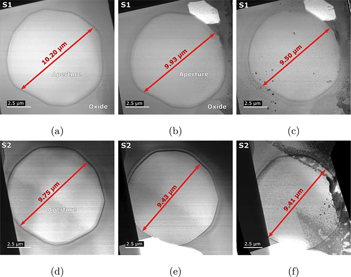
In-situ observation of lateral AlAs oxidation and dislocation formation in VCSELs
R. Fabbro, R. Coppeta, M. Pusterhofer, G. Fasching, T. Haber, W. Grogger
Understanding how defects are generated and propagate during operation in modern vertical cavity surface emitting lasers (VCSEL) is an important challenge in order to develop the next generation of highly reliable semiconductor lasers. Undesired oxidation processes or performance degrading dislocation networks are typically investigated by conventional failure analysis after damage formation. In this works new approach to VCSEL failure analysis, oxide confined high power VCSELs are investigated in-situ at elevated temperatures in a transmission electron microscope. At high temperatures, lateral oxidation of the current confinement layer as well as formation and propagation of dislocations are observed. The experimental results may deepen the understanding of defect generation in VCSELs during stress tests or standard operating conditions. On the other hand, in-situ TEM proofed to be a promising technique to be utilised in future VCSEL failure analysis, possibly leading to the development of improved defect models and increased VCSEL reliability.