The Quanta 3D FEG is a combined scanning electron / focused ion beam microscopy (SEM and FIB, respectively) with variable operation in high-, low- (10 – 130 Pa) and extended low-vacuum (up to 4000 Pa), summarized in the term environmental SEM (ESEM). This installation is optimized for additive direct-write fabrication of functional micro- and nanostructures using focused ion / electron beam induced deposition (FIBID / FEBID) with particular focus on 3D nano-printing. FIB processing down to 2 kV and 1 pA is also available, which complements rapid prototyping for a broad range of materials not least due to the low- and environmental-vacuum options. Furthermore, the system is equipped with micro- / nano-manipulation devices and allows installation of low- and high-temperature stages (5° – 800 °C). In near future, the system will be expanded by an in situ atomic force microscope (AFSEM® by GETec Microscopy Inc., Vienna, Austria) to enable correlated microscopy by combining the individual capabilities of the microscope for a comprehensive insight in materials and functionalities down to the nanoscale.
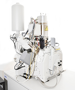
FIB / (E)SEM Dual Beam Microscope Quanta 3D FEG
Key Features
- Dual beam conception for (simultaneous) electron and ion beam processing
- High resolution imaging via both beams (SEM / FIB)
- Additive direct-write fabrication of electrically conductive / insulating, magnetic or optically active micro- and nanostructures via focused electron / ion beam induced deposition (FEBID / FIBID)
- Particular focus on direct-write 3D nano-printing via FEBID / FIBID
- Subtractive fabrication of micro- and nanostructures via FIB processing
- Low temperature processing using a peltier stage (down to ~ 5°C)
- High temperature processing using heating MEMS (up to 800°C)
- Micro- and nano-manipulation option
- In situ AFM for correlated microscopy (3D morphology and specific functionality)
Essential Specifications
Emitter & Resolution
- SEM
- Type: thermal field emission gun (FEG)
- Primary electron energies: 0.5 keV – 30 keV
- Beam currents: 0.7 pA – 5 µA
- Resolution:
- 2 nm @ 30 keV
- 5 nm @ 30 keV (low-vacuum mode)
- 5 nm @ 30 keV (extended low-vacuum mode)
- 9 nm @ 1 keV
- 9 nm @ 3 keV (low-vacuum mode)
- FIB
- Type: Ga+ liquid ion metal source (LIMS)
- Primary ion energies: 2 kV – 30 kV
- Beam currents: 1 pA – 65 nA
- Resolution: < 7 nm @ 30 kV (eucentric)
Additive / Subtractive Manufacturing
- 4 fixed gas injection systems, providing deposition of Pt, Au, Fe and SiO2
- 1 variable gas injection system (Kleindiek) for precursor testing including the possibility of external carrier gas injection
- FEBID performance (additive)
- Minimum line widths < 13 nm (FWHM) at heights of 20 nm (for Pt on Si)
- Freestanding 3D architectures with minimum feature widths < 30 nm (for Au)
- FIBID performance (additive)
- Minimum line widths < 40 nm (for Pt on Si)
- Freestanding 3D architectures with minimum feature widths < 70 nm (for Pt)
- FIB performance (subtractive)
- < 15 nm line width
- ~ 20:1 height:width ratio
Detectors & Stage & Add-Ons
- Everhart Thornley SE / BSE Detector (latter via grid voltages)
- Embedded sample current measurements (software integrated & external)
- XYZ stage movement: 50 mm / 50 mm / 25 mm
- Rotation: 360° (continuous) with < 1 µm repeatability
- Tilt: -15° – 75° (ion beam tilted 52° w.r.t. electron beam)
- Micromanipulation (Kleindiek)
- Electric nanoprobing
- Nanomanipulation (movement / transfer)
- Rotation needle option
- Nano-grabber option
- Low temperature stage
- Peltier element (40×40 mm)
- Operation range 5 °C – 40 °C
- High temperature stage
- Chip holder for DensSolution heating chips
- Operation temperatures up to 800°C
- Active closed loop operation including temperature profile option