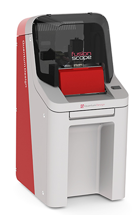
Although Scanning Electron Microscopy (SEM) and Atomic Force Microscopy (AFM) provides highly complementary information, there were no deeply integrated systems available on the market for a very long time. The reason for that might be found in the space requirements for classical AFM instrumentation, foremost laser / detection units, which are complicated to be integrated in space confined SEM vacuum chambers. As alternative, different add-on AFMs were sometimes retro-fitted to SEM host systems, which basically worked (e.g. the AFSEM®), but after all, remained the character of two separate systems with technical and practical limitations. Based on that motivation, GETec Microscopy Inc. joined forces with Quantum Design Microscopy and started a radically new development, which was officially launched in September 2022: the FUSIONScope™ (see right / left). That system fills the gap of a deeply integrated SEM-AFM solution and leverages the area of correlated microscopy to a truly new level. The first system worldwide was delivered to FELMI-ZFE, where we use the possibilities for situations, where stand-alone AFMs run into their intrinsic limitations. Below, an inside illustration of the concept is shown together with a few examples (circles), where SEM-assisted AFM positioning is not optional but decisive.
FUSIONScope™
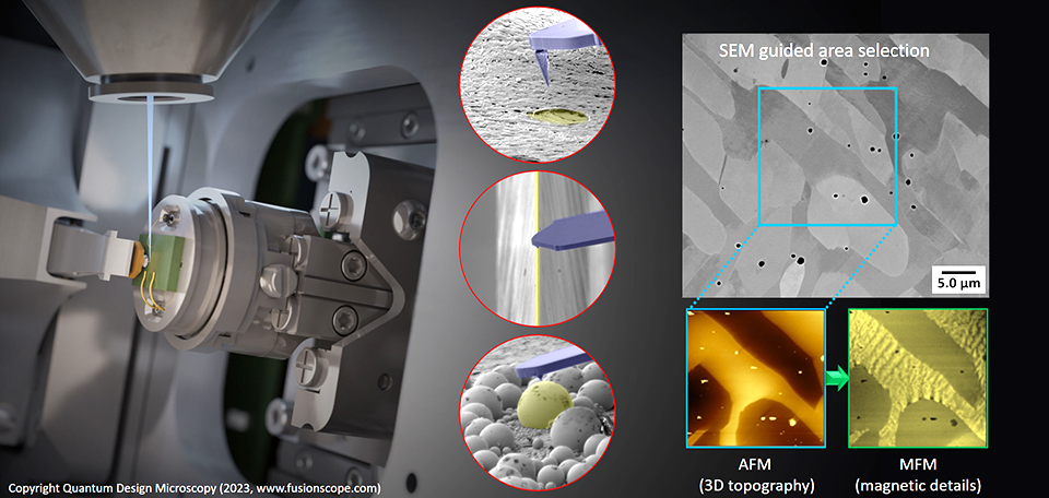
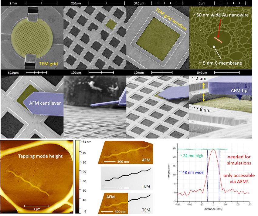
The combined workflow starts with the precise, SEM-based identification of relevant regions via inspection from top, but in particular via side-view imaging at angles up to 80°. By that, the AFM tip can be exactly placed on even challenging regions, as shown in the two upper rows of the figure below. The FUSIONScope™ then provides a wide range of operation modes, including contact-mode, tapping-mode, phase-mode, conductive-AFM (CAFM), electrostatic force microscopy (EFM), magnetic force microscopy (MFM) and nanomechanical mapping (FIRE-mode) for a comprehensive surface evaluation. A representative example is shown in the bottom row for additively written Au nanowire, placed on a sub-5 nm thick carbon membrane to enable transmission electron microscopy (TEM) measurements. As evident, the system is very sensitive even on such challenging substrates, as shown by the direct comparison to TEM measurements, where AFM provides complementary, quantitative cross-sectional profiles. In the previous figure, a correlated SEM-AFM-MFM example is shown, which illustrates the highly complementary character of the applied techniques by accessing crystalline peculiarities(SEM), surface morphologies (AFM) and magnetic details (MFM) for comprehensive insights.
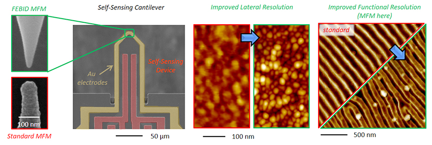
In a strong collaboration with both manufacturer companies, FELMI-ZFE was not only involved in the actual system development but still contributes with advanced 3D nano-probe concepts in the frame of the Christian Doppler Laboratory DEFINE. By application of the 3D nanoprinting technology Focused Electron Beam Induced Deposition (FEBID [1]) on pre-finished self-sensing cantilevers, novel conceptsare realized, which leverages CAFM, EFM [2], and MFM [3] characterization to a truly new level [4], as representatively shown below (more details can be found here). By that, the FUSIONScope™ is an ideal platform for situations where both, SEM and AFM, are indispensably needed to obtain correlated material insights. In particular, very challenging surface morphologies or highly localized regions benefit from the SEM possibilities due to the complementary character and the technological advances provided by the FUSIONScope™. Together with the unique nano-probes developed here, the system indeed opens up a new chapter in correlated microscopy.
[1] 3D Nanoprinting via Focused Electron Beams. Robert Winkler et al.; Journal of Applied Physics 2019, 125 (21), 210901.
[2] 3D Nanoprinting of All-Metal Nanoprobes for Electric AFM Modes. Lukas M. Seewald et al.; Nanomaterials 2022, 12 (24), 4477.
[3] Additive Manufacturing of Co3Fe Nano-Cones for Magnetic Force Microscopy. Robert Winkler and Michele Brugger-Hatzl et al.; Nanomaterials 2023, 13, 1217.
[4] i) Focused Electron Beam-Based 3D Nanoprinting for Scanning Probe Microscopy: A Review. Harald Plank et al., Micromachines2019, 11 (1), 48.
[4] ii)Three-Dimensional Nanothermistors for Thermal Probing. Jürgen Sattelkow et al.; ACS Appl. Mat. Interf.2019, 11 (25), 22655.